Adisyn’s Graphene Gambit: Could This ASX Small Cap Be the One to Displace Copper in the Chip Race?

In the semiconductor world, the smallest connections often carry the biggest implications. For over two decades, copper has been the interconnect material of choice, faithfully carrying electrical signals across ever-smaller chip designs. But as transistors shrink beyond the 5nm threshold and data demands surge, copper is increasingly looking like yesterday’s metal.
This morning, Adisyn (ASX: AI1) entered the next phase of a project that, if successful, could make the industry’s reliance on copper a thing of the past. Through its Israeli-based subsidiary, 2D Generation, the company announced that its low-temperature graphene interconnect program has formally entered Phase One development, backed by a newly commissioned Atomic Layer Deposition (ALD) system in Israel and parallel testing underway at Tel Aviv University.
It’s a highly technical step — but one with global ramifications if proven at scale.

Adisyn’s Beneq TFS 200 ALD system
The Interconnect Problem Nobody Talks About
While chip designers have stretched Moore’s Law to the limits, interconnects — the fine metal lines linking transistors — have become a quiet constraint. Copper, though excellent in bulk, suffers from increased resistance and heat generation at nanoscale widths. This slows signal transmission and consumes more power — neither of which suits the AI-drenched future the sector is heading towards.
Graphene, a one-atom-thick sheet of carbon, offers an enticing alternative. It boasts far superior electrical and thermal conductivity, without copper’s scaling drawbacks. But the catch has always been fabrication. The industry has struggled to grow high-quality graphene films directly onto wafers at temperatures compatible with existing semiconductor processes.
That’s precisely the nut Adisyn is trying to crack.
What’s New in Today’s Announcement?
Adisyn’s update confirms the operational readiness of its Beneq TFS 200 ALD system, a platform customised for precision thin-film deposition. The system is now being used to conduct the first phase of graphene growth — a complex, multi-step process designed to validate the company’s proprietary low-temperature deposition method.
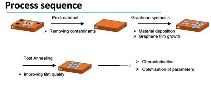
The process is more than just laying down atoms. It involves:
Plasma Pre-Clean: Preparing the wafer by removing surface contaminants to allow for uniform film growth.
Deposition Sequence: Reacting selected organic precursors with gases to form initial graphene layers.
Post-Anneal: A thermal treatment that improves the crystalline quality and conductivity of the film.
Characterisation and Feedback: Rigorous testing of each layer to optimise deposition parameters in an iterative loop.
Multiple precursor materials are being trialled through this cycle. If successful, the project will progress to Phase Two in early 2026, focused on wafer-scale integration and commercial collaboration.
Small Cap, Global Ambition
For an ASX microcap, Adisyn is operating in surprisingly elite company. Its R&D efforts are underpinned by partnerships with Tel Aviv University, imec in Belgium — a leading European nanoelectronics research hub — and the EU-backed “Connecting Chips” program, alongside names such as NVIDIA, Applied Materials, and NXP.
The program is led by a heavyweight team, including:
Chairman Kevin Crofton, formerly of Lam Research and SPTS Technologies.
Arye Kohavi, CEO of 2D Generation, best known for founding the atmospheric water company Water-Gen.
Paul Rich, a respected semiconductor technologist with deep expertise in wafer-scale processing and plasma deposition.
Miri Kish Dagan, ex-Tower Semiconductors, who brings decades of advanced materials engineering experience.
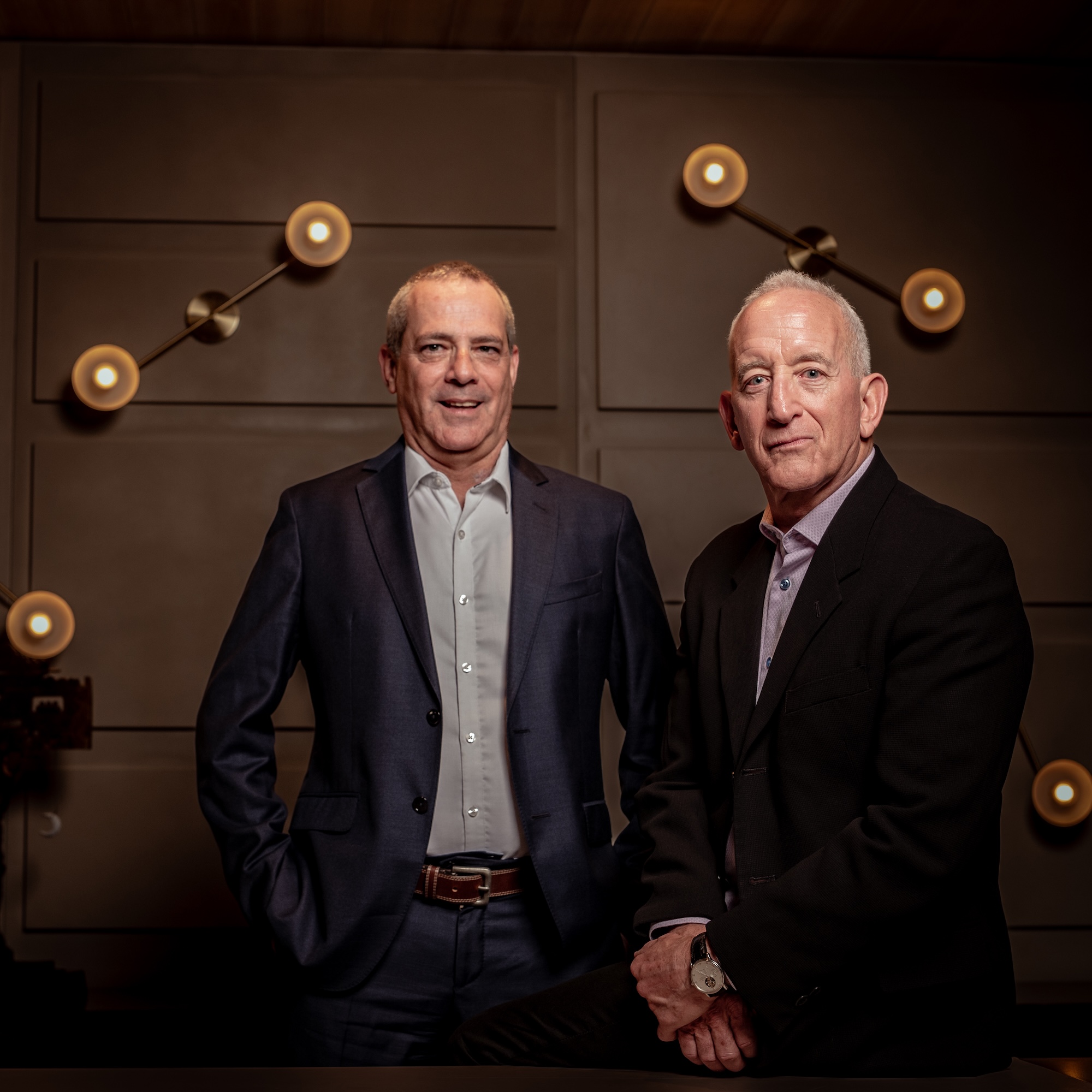
Kevin Crofton and Arye Kohavi
Kohavi, not known for understatement, was clear on the significance:
“This is not just about performance — it’s about scalability, sustainability, and what’s possible at the atomic level. If we can validate graphene deposition in a repeatable, cost-effective way, it could become foundational across AI, data, and communications infrastructure.”
Why It Matters to the Sector
If Adisyn’s process works — and that’s still an “if” — the implications could be profound. A scalable, low-temperature graphene interconnect solution would offer foundries a path to continue shrinking chips and boosting performance without a complete retooling of their fab infrastructure.
With Moore’s Law nearing its commercial and physical limits, new materials are no longer optional — they’re essential. Governments, too, are watching. The US CHIPS Act, the EU’s semiconductor sovereignty push, and similar programs in Korea and Japan are all looking for advanced process breakthroughs that can restore or protect competitive advantage.
A validated graphene process, particularly one licensable and fab-compatible, would put Adisyn on the radar of major industry players.
Still Early — But Now It’s Real
To be clear, Adisyn remains early in the journey. The project is pre-revenue, technical risk remains, and wafer-scale reproducibility is a long road from laboratory success. But it’s no longer just a concept on paper. The hardware is installed. The process is running. And the partners are watching.
In a sector where change tends to come from billion-dollar R&D labs in the US, Korea or Taiwan, it’s not often an ASX-listed small cap throws its hat into the ring — let alone with a credible shot at success.
Copper might not be out just yet. But thanks to Adisyn, graphene is no longer just a story of promise. It’s becoming a real competitor.
This article does not constitute financial advice. Readers should seek advice from appropriate advisors before making an investment decision and always do their own research.