Adisyn Powers Up: Graphene Dreams Edge Closer as New ALD System Goes Live

In the quest for the holy grail of next-gen semiconductors, Adisyn Ltd (ASX: AI1) has flicked the switch on a critical piece of hardware at its 2D Generation (2DG) facility in Israel. The successful commissioning of a state-of-the-art Atomic Layer Deposition (ALD) system marks a decisive step forward in the company’s mission to create scalable, low-temperature graphene interconnects for high-performance chips.
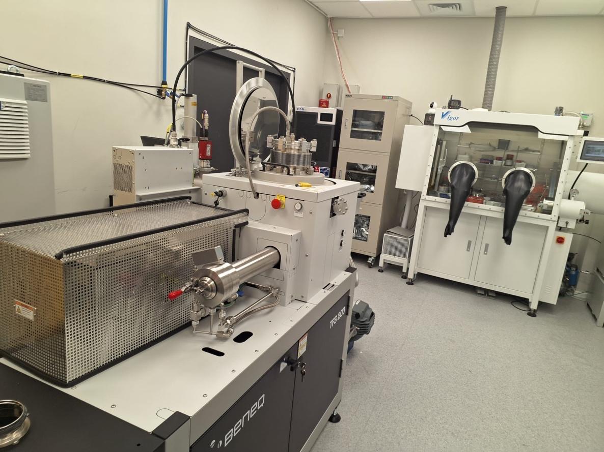
Tucked away in the Yakum Industrial Park, this newly installed Beneq TFS 200 system isn’t just a fancy lab toy—it’s a linchpin for 2DG’s proprietary process that aims to sidestep traditional semiconductor barriers with atom-thin precision.
“Commissioning this new ALD system represents a major operational leap for Adisyn,” declared chairman Kevin Crofton. “The precision, flexibility, and throughput of this platform enables us to rigorously test our graphene interconnect solution under real-world semiconductor conditions.”
And it’s not going it alone. A twin Beneq unit housed at Tel Aviv University’s Jan Koum Center will operate in tandem, allowing parallel testing—a classic divide-and-conquer strategy in R&D.
So, why all the fuss over a deposition tool? In the semiconductor world, ALD systems are the unsung heroes responsible for layering materials with atomic-level precision. The Beneq TFS 200, in particular, comes decked out with upgrades tailor-made for graphene experimentation: plasma capabilities for surface treatments, a semi-automatic load lock for quick sample swaps at room temperature, and a reaction chamber that supports wafer-scale processing.
According to the company, the benefits over its legacy system are substantial: broader temperature thresholds, enhanced process control, and throughput that promises to shift development into top gear. It’s like swapping your family sedan for a Formula 1 car—if your family car also made microchips.
This latest advancement is underpinned by recent infrastructure upgrades to the Israeli facility, including enhanced environmental controls and bespoke electrical systems. It’s a reminder that cutting-edge science isn’t just about having the right ideas—it’s about having the right environment to execute them.
The ultimate goal? A low-temperature graphene deposition method that could transform the semiconductor interconnect game. Current copper interconnects face heat and scaling challenges as chips shrink and speeds increase. Graphene, with its legendary conductivity and strength, offers a tantalising alternative—but only if it can be reliably and affordably integrated into chip designs.
Adisyn, through 2D Generation, is chasing that integration with gusto. The newly commissioned setup will not only validate past results but broaden the experimental canvas, enabling testing across various substrates and layer structures. A development roadmap update is slated for Q1 FY26, likely providing a clearer view of how close the company is to cracking the graphene conundrum.
Founded by Arye Kohavi, 2DG operates with an eye on broader industry shifts in AI, data storage, telecommunications, and cybersecurity—all sectors hungry for faster, smaller, and more efficient chips.
While Adisyn remains best known for its managed technology services here in Australia, its ambitions through 2DG are boldly global. By investing in the materials science frontier, the company is positioning itself not just as a solutions provider but as a potential innovator in the silicon-steeped corridors of the semiconductor world.
Whether graphene will ultimately dethrone copper in chip design remains to be seen. But with a high-spec ALD system humming away in Israel—and its twin spinning in Tel Aviv—Adisyn looks well placed to give the material a fighting chance.